- 您现在的位置:买卖IC网 > Sheet目录342 > MCB1114 (Keil)BOARD EVALUATION FOR NXP LPC1114
�� �
�
�NXP� Semiconductors�
�LPC1111/12/13/14�
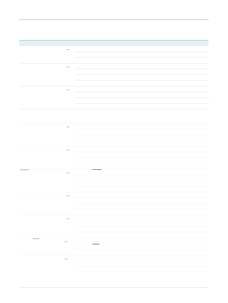
�Table� 4.�
�LPC1114� pin� description� table� (PLCC44� package)� …continued�
�Symbol�
�PIO0_9/MOSI0/�
�CT16B0_MAT1�
�SWCLK/PIO0_10/�
�SCK0/CT16B0_MAT2�
�TDI/PIO0_11/�
�AD0/CT32B0_MAT3�
�PIO1_0� to� PIO1_11�
�Pin�
�32� [1]�
�33� [1]�
�36� [3]�
�Type�
�I/O�
�I/O�
�O�
�I�
�I/O�
�I/O�
�O�
�I�
�I/O�
�I�
�O�
�I/O�
�Description�
�PIO0_9� —� General� purpose� digital� input/output� pin.�
�MOSI0� —� Master� Out� Slave� In� for� SPI0.�
�CT16B0_MAT1� —� Match� output� 1� for� 16-bit� timer� 0.�
�SWCLK� —� Serial� wire� clock� and� test� clock� TCK� for� JTAG� interface.�
�PIO0_10� —� General� purpose� digital� input/output� pin.�
�SCK0� —� Serial� clock� for� SPI0.�
�CT16B0_MAT2� —� Match� output� 2� for� 16-bit� timer� 0.�
�TDI� —� Test� Data� In� for� JTAG� interface.�
�PIO0_11� —� General� purpose� digital� input/output� pin.�
�AD0� —� A/D� converter,� input� 0.�
�CT32B0_MAT3� —� Match� output� 3� for� 32-bit� timer� 0.�
�Port� 1� —� Port� 1� is� a� 12-bit� I/O� port� with� individual� direction� and� function�
�controls� for� each� bit.� The� operation� of� port� 1� pins� depends� on� the� function�
�selected� through� the� IOCONFIG� register� block.�
�TMS/PIO1_0/�
�AD1/CT32B1_CAP0�
�TDO/PIO1_1/�
�AD2/CT32B1_MAT0�
�TRST/PIO1_2/�
�AD3/CT32B1_MAT1�
�SWDIO/PIO1_3/AD4/�
�CT32B1_MAT2�
�PIO1_4/AD5/�
�CT32B1_MAT3/WAKEUP�
�PIO1_5/RTS/�
�CT32B0_CAP0�
�PIO1_6/RXD/�
�CT32B0_MAT0�
�37� [3]�
�38� [3]�
�39� [3]�
�41� [3]�
�42� [3]�
�2� [1]�
�3� [1]�
�I�
�I/O�
�I�
�I�
�O�
�I/O�
�I�
�O�
�I�
�I/O�
�I�
�O�
�I/O�
�I/O�
�I�
�O�
�I/O�
�I�
�O�
�I�
�I/O�
�O�
�I�
�I/O�
�I�
�TMS� —� Test� Mode� Select� for� JTAG� interface.�
�PIO1_0� —� General� purpose� digital� input/output� pin.�
�AD1� —� A/D� converter,� input� 1.�
�CT32B1_CAP0� —� Capture� input� 0� for� 32-bit� timer� 1.�
�TDO� —� Test� Data� Out� for� JTAG� interface.�
�PIO1_1� —� General� purpose� digital� input/output� pin.�
�AD2� —� A/D� converter,� input� 2.�
�CT32B1_MAT0� —� Match� output� 0� for� 32-bit� timer� 1.�
�TRST� —� Test� Reset� for� JTAG� interface.�
�PIO1_2� —� General� purpose� digital� input/output� pin.�
�AD3� —� A/D� converter,� input� 3.�
�CT32B1_MAT1� —� Match� output� 1� for� 32-bit� timer� 1.�
�SWDIO� —� Serial� wire� debug� input/output.�
�PIO1_3� —� General� purpose� digital� input/output� pin.�
�AD4� —� A/D� converter,� input� 4.�
�CT32B1_MAT2� —� Match� output� 2� for� 32-bit� timer� 1.�
�PIO1_4� —� General� purpose� digital� input/output� pin.�
�AD5� —� A/D� converter,� input� 5.�
�CT32B1_MAT3� —� Match� output� 3� for� 32-bit� timer� 1.�
�WAKEUP� —� Deep� power-down� mode� wake-up� pin.�
�PIO1_5� —� General� purpose� digital� input/output� pin.�
�RTS� —� Request� To� Send� output� for� UART.�
�CT32B0_CAP0� —� Capture� input� 0� for� 32-bit� timer� 0.�
�PIO1_6� —� General� purpose� digital� input/output� pin.�
�RXD� —� Receiver� input� for� UART.�
�LPC1111_12_13_14_0�
�O�
�CT32B0_MAT0� —� Match� output� 0� for� 32-bit� timer� 0.�
�?� NXP� B.V.� 2009.� All� rights� reserved.�
�Objective� data� sheet�
�Rev.� 00.11� —� 13� November� 2009�
�12� of� 53�
�发布紧急采购,3分钟左右您将得到回复。
相关PDF资料
MCB11C14
BOARD EVAL FOR NXP LPC11C14
MCB2470
BOARD EVAL NXP LPC247X SERIES
MCBSTM32EXL
BOARD EVALUATION FOR STM32F103ZE
MCBTMPM330
BOARD EVAL TOSHIBA TMPM330 SER
MCIMX25WPDKJ
KIT DEVELOPMENT WINCE IMX25
MCIMX53-START-R
KIT DEVELOPMENT I.MX53
MCM69C432TQ20
IC CAM 1MB 50MHZ 100LQFP
MCP1401T-E/OT
IC MOSFET DRVR INV 500MA SOT23-5
相关代理商/技术参数
MCB1114-ED
制造商:ARM Ltd 功能描述:KEIL NXP LPC1114 EVAL BOARD
MCB1114U
功能描述:开发板和工具包 - ARM EVAL BOARD FOR NXP LPC1114 + ULINK2
RoHS:否 制造商:Arduino 产品:Development Boards 工具用于评估:ATSAM3X8EA-AU 核心:ARM Cortex M3 接口类型:DAC, ICSP, JTAG, UART, USB 工作电源电压:3.3 V
MCB1114U-ED
制造商:ARM Ltd 功能描述:KEIL NXP LPC1114 EVAL BOARD
MCB1114UME
功能描述:开发板和工具包 - ARM EVAL BOARD FOR NXP LPC1114 + ULINK-ME
RoHS:否 制造商:Arduino 产品:Development Boards 工具用于评估:ATSAM3X8EA-AU 核心:ARM Cortex M3 接口类型:DAC, ICSP, JTAG, UART, USB 工作电源电压:3.3 V
MCB1114UME-ED
制造商:ARM Ltd 功能描述:KEIL NXP LPC1114 EVAL BOARD
MCB11C14
功能描述:开发板和工具包 - ARM EVAL BOARD FOR NXP LPC11C14
RoHS:否 制造商:Arduino 产品:Development Boards 工具用于评估:ATSAM3X8EA-AU 核心:ARM Cortex M3 接口类型:DAC, ICSP, JTAG, UART, USB 工作电源电压:3.3 V
MCB11C14-ED
制造商:ARM Ltd 功能描述:KEIL NXP LPC11C14 EVAL BOARD
MCB11C14U
功能描述:开发板和工具包 - ARM EVAL BOARD FOR NXP LPC11C14 + ULINK2
RoHS:否 制造商:Arduino 产品:Development Boards 工具用于评估:ATSAM3X8EA-AU 核心:ARM Cortex M3 接口类型:DAC, ICSP, JTAG, UART, USB 工作电源电压:3.3 V